A phase may be defined as a homogeneous portion of a system that has uniform physical and chemical characteristics. Every pure material is considered to be a phase; so also is every solid, liquid, and gaseous solution. For example, a sugar–water syrup solution is one phase, and solid sugar is another. Each has different physical properties (one is a liquid, the other is a solid); furthermore, each is different chemically (i.e., has a different chemical composition); one is virtually pure sugar, the other is a solution of H2O and C12H22O11.
If more than one phase is present in a given system, each will have its own distinct properties, and a boundary separating the phases will exist across which there will be a discontinuous and abrupt change in physical and/or chemical characteristics. When two phases are present in a system, it is not necessary that there be a difference in both physical and chemical properties; a disparity in one or the other set of properties is sufficient. When water and ice are present in a container, two separate phases exist; they are physically dissimilar (one is a solid, the other is a liquid) but identical in chemical makeup.
Also, when a substance can exist in two or more polymorphic forms (different arrangements of the atoms, as in two different crystalline structures), each of these structures is a separate phase because their respective physical characteristics differ, and this difference can be measured in the form of a macroscopic variable, like conductivity or magnetization.
Phase transitions are ubiquitous in science, from fundamental physics, chemistry, or biology to ecological or even social systems. These transitions have a broad range of applications, from data storage to drug delivery. Phase transitions manifest themselves as changes, as we have noted, of a macroscopic physical characteristic.
For a detailed understanding of the different phases as well as the mechanism of phase transitions, knowledge about the individual objects is required. Various techniques based on microscopy or diffraction have been applied to analyse the structure of different phases.
The case of the arrangement of adsorbates on a surface is especially important in technological and fundamental research. It is is governed by interactions between the adsorbate and the atoms of the supporting surface as well as between the adsorbates themselves. The geometric structure these adsorbates assemble into can be studied by ensemble averaging techniques like electron diffraction or real space imaging techniques like low electron energy microscopy (LEEM), electron microscopy, scanning tunneling microscopy (STM), and atomic force microscopy (AFM).
These latter two techniques (STM and AFM) allow for the determination of the positions of individual atoms or molecules on the atomic scale. Not only that, the tip of an STM or AFM may act as a local probe to provide a stimulus to induce phase changes.
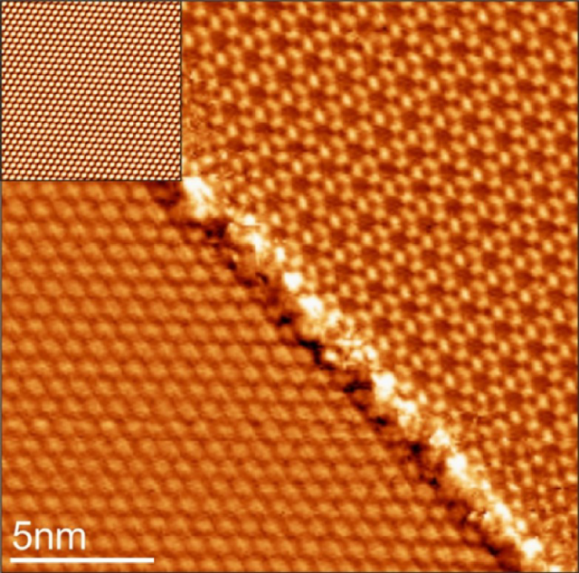
Now, Nicolás Lorente, from DIPC and ICM, and a team of researchers have used1 the tip of an STM to induce a structural phase transition between two phases of a monolayer of CO on a Cu(111) surface (see Figure 1). The reversible transitions between phases are caused by the electric field between the tip and the sample surface.
The experiments reveal a structural 2D phase transition between two rather complex molecular arrangements of CO on Cu(111), which is reversible despite the slightly different coverages. Because the transition is efficiently triggered by the electric field of an STM tip using voltages in the range of ±3 V, it opens a new field of research, especially due to the excellent control of the experimental conditions.

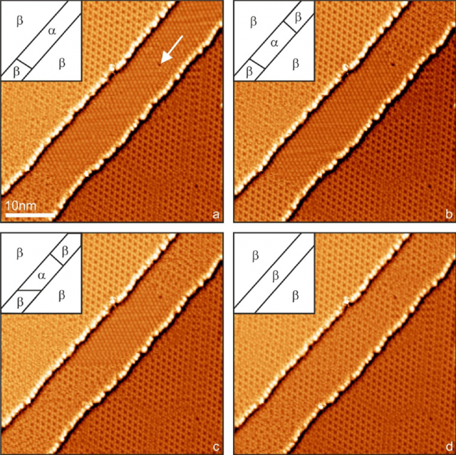
In contrast to thermally induced transitions, the researchers found that very localized areas can be reversibly transformed and patterns of the two phases may be written on a small scale (see Figure 2) and that the switching times can be very fast.
It is remarkable that, in contrast to the common observation of phase transitions, not only macroscopic quantities of a large ensemble may be studied but also the position of every element of the system can be directly accessed. Given the ease of the experiment, it is an ideal model system to be used to better understand the physics of structural phase transitions on the atomic scale.
References
- B. Wortmann , D. van Vörden, P. Graf, R. Robles, P. Abufager, N. Lorente, C. A. Bobisch, and R. Möller (2016) Reversible 2D Phase Transition Driven By an Electric Field: Visualization and Control on the Atomic Scale Nano Letters DOI: 10.1021/acs.nanolett.5b04174 ↩
No comments:
Post a Comment